Summary
The PiezoMAT team |  |
The European project PIEZOMAT proposes a new technology of very high-resolution fingerprint sensors based on a matrix of interconnected piezoelectric ZnO nanowires (NWs).
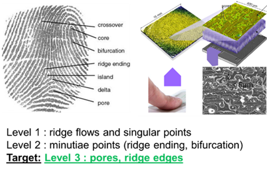
The direct consequence of integrating nano-objects on microelectronic chips rather than conventional microsystems is to diminish the size of individual pixels, which enables larger integration densities and thus higher spatial resolutions (>1000 dpi).
PiezoMATexplores 3 possible configurations with the charge collections at the bottom of single nanowires or with top-bottom contacts.
Partners challenges were the integration of ZnOnanowires, onto microelectronics chips (200mm wafer), considering process compatibility at the wafer scale of the successive nanowire growth, contacting and encapsulation steps.

Principle
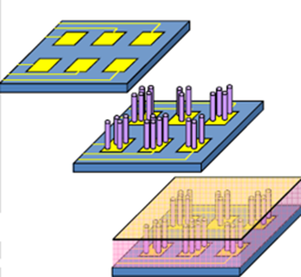
- Each nanowire or bundle of nanowires forms a pixel (size below 50 × 50 µm2)
- Pixel encapsulated in a polymer
- Generated potentials are proportional to the NW displacement

- Nanowire growth
- Encapsulation
- Top electrode
- Bonding
- Testing
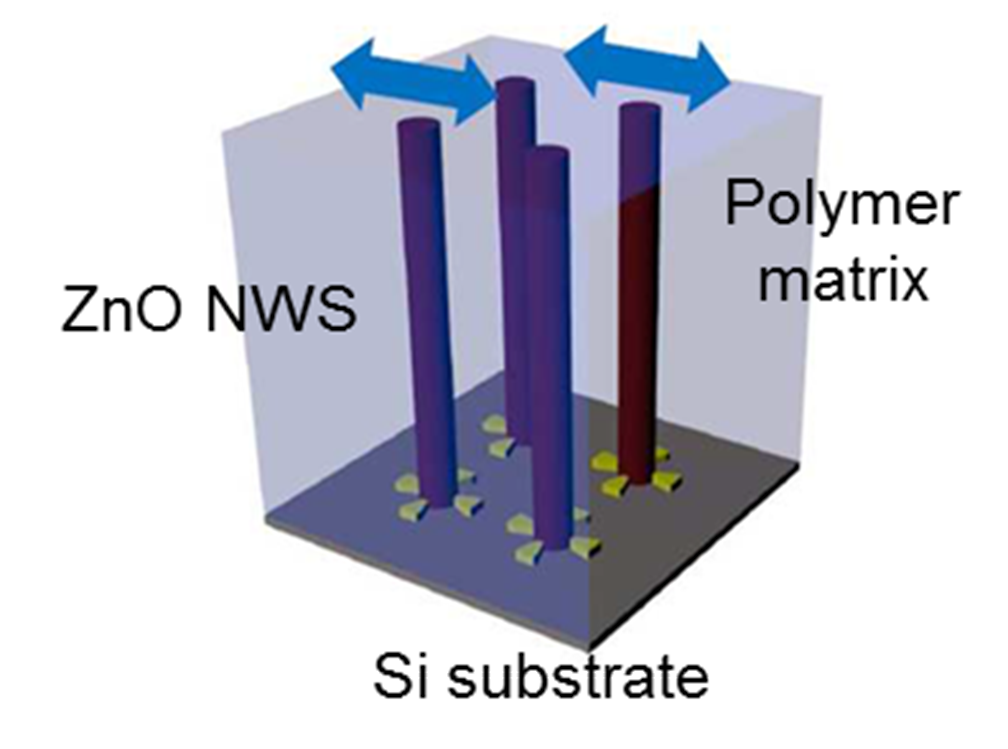
- 2 contacts in high potential area
- 5000dpi – 8 × 8 pixels
- Technologically challenging
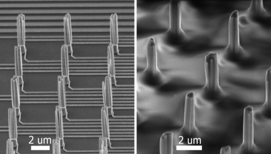
- First experimental demonstration of bottom-bottom contacted 'bending mode’ force sensor
- Very high gauge factor and force sensitivity on the active NWs
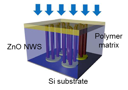
- 2 top-bottom contacts
- 1000dpi – 25 × 10 pixels
- Technologically safer
- Development of stable and reproducible process in clean-room
- Successful NWs integration: localized and contacted NWs growth on a processed 200 mm silicon wafer
- Development of a suitable UV-crosslinkable polymeric formulation and an accurate deposition process for the encapsulation
- Development of highly conductive top electrodes
- Demonstration of the feasibility of the compression option → full device setup for MORPHO’s application
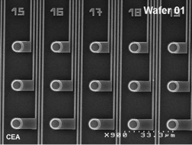
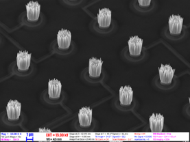
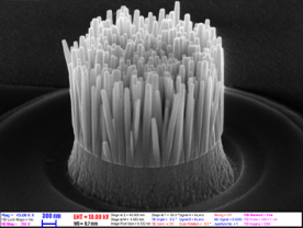
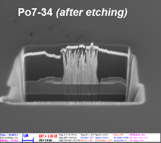
Results - Conclusions
- Morpho: peak response to mechanical contact (250 pixels)
- MFA: pattern recognition and position sensitivity (128 pixels, one by one)
- Fraunhofer: the 8-bit detection is successfully demonstrated (80 pixels)
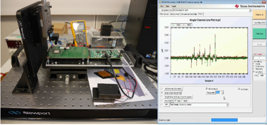
Morpho characterisation: peak respons of 250 pixels

MFA characterisation: position sensitive pattern recognition by 128 pixels

